
This VHDL post presents a VHDL code for a single-port RAM (Random Access Memory). The VHDL testbench code is also provided to test the single-port RAM in Xilinx ISIM. The RAM's size is 128x8 bit.
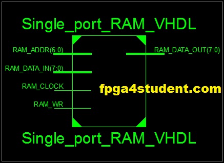
As shown in the figure above, the 128x8 single port RAM in VHDL has following inputs and outputs:
1. RAM_CLOCK: the clock signal for sequentially writing data to the single-port RAM.
2. RAM_DATA_IN: 8-bit input data to be written to RAM at the provided input address RAM_ADDR when it is enabled.
3. RAM_WR: Write enable signal for writing to RAM, only if RAM_WR = 1, RAM_DATA_IN is written to the RAM at the rising edge of the clock signal.
4. RAM_ADDR: 6-bit Address where 8-bit input data are written to and data are read out.
5. RAM_DATA_OUT: 8-bit output data read out from the provided input address RAM_ADDR.
VHDL code for the single-port RAM:
-- fpga4student.com: FPGA projects, Verilog projects, VHDL projects
-- VHDL project: VHDL code for a single-port RAM
library IEEE;
use IEEE.STD_LOGIC_1164.ALL;
USE ieee.numeric_std.ALL;

-- A 128x8 single-port RAM in VHDL
entity Single_port_RAM_VHDL is
port(
 RAM_ADDR: in std_logic_vector(6 downto 0); -- Address to write/read RAM
 RAM_DATA_IN: in std_logic_vector(7 downto 0); -- Data to write into RAM
 RAM_WR: in std_logic; -- Write enable
 RAM_CLOCK: in std_logic; -- clock input for RAM
 RAM_DATA_OUT: out std_logic_vector(7 downto 0) -- Data output of RAM
);
end Single_port_RAM_VHDL;

architecture Behavioral of Single_port_RAM_VHDL is
-- define the new type for the 128x8 RAM
type RAM_ARRAY is array (0 to 127 ) of std_logic_vector (7 downto 0);
-- initial values in the RAM
signal RAM: RAM_ARRAY :=(
   x"55",x"66",x"77",x"67",-- 0x00:
   x"99",x"00",x"00",x"11",-- 0x04:
   x"00",x"00",x"00",x"00",-- 0x08:
   x"00",x"00",x"00",x"00",-- 0x0C:
   x"00",x"00",x"00",x"00",-- 0x10:
   x"00",x"00",x"00",x"00",-- 0x14:
   x"00",x"00",x"00",x"00",-- 0x18:
   x"00",x"00",x"00",x"00",-- 0x1C:
   x"00",x"00",x"00",x"00",-- 0x20:
   x"00",x"00",x"00",x"00",-- 0x24:
   x"00",x"00",x"00",x"00",-- 0x28:
   x"00",x"00",x"00",x"00",-- 0x2C:
   x"00",x"00",x"00",x"00",-- 0x30:
   x"00",x"00",x"00",x"00",-- 0x34:
   x"00",x"00",x"00",x"00",-- 0x38:
   x"00",x"00",x"00",x"00",-- 0x3C:
   x"00",x"00",x"00",x"00",-- 0x40:
   x"00",x"00",x"00",x"00",-- 0x44:
   x"00",x"00",x"00",x"00",-- 0x48:
   x"00",x"00",x"00",x"00",-- 0x4C:
   x"00",x"00",x"00",x"00",-- 0x50:
   x"00",x"00",x"00",x"00",-- 0x54:
   x"00",x"00",x"00",x"00",-- 0x58:
   x"00",x"00",x"00",x"00",-- 0x5C:
   x"00",x"00",x"00",x"00",
   x"00",x"00",x"00",x"00",
   x"00",x"00",x"00",x"00",
   x"00",x"00",x"00",x"00",
   x"00",x"00",x"00",x"00",
   x"00",x"00",x"00",x"00",
   x"00",x"00",x"00",x"00",
   x"00",x"00",x"00",x"00"
   );
begin
process(RAM_CLOCK)
begin
 if(rising_edge(RAM_CLOCK)) then
 if(RAM_WR='1') then -- when write enable = 1,
 -- write input data into RAM at the provided address
 RAM(to_integer(unsigned(RAM_ADDR))) <= RAM_DATA_IN;
 -- The index of the RAM array type needs to be integer so
 -- converts RAM_ADDR from std_logic_vector -> Unsigned -> Interger using numeric_std library
 end if;
 end if;
end process;
 -- Data to be read out
 RAM_DATA_OUT <= RAM(to_integer(unsigned(RAM_ADDR)));
end Behavioral;
VHDL Testbench code for the single-port RAM:
-- fpga4student.com: FPGA projects, Verilog projects, VHDL projects
-- VHDL project: VHDL code for a single-port RAM
LIBRARY ieee;
USE ieee.std_logic_1164.ALL;
USE ieee.std_logic_unsigned.ALL;
-- VHDL testbench code for the single-port RAM
ENTITY tb_RAM_VHDL IS
END tb_RAM_VHDL;

ARCHITECTURE behavior OF tb_RAM_VHDL IS

    -- Component Declaration for the single-port RAM in VHDL

    COMPONENT Single_port_RAM_VHDL
    PORT(
         RAM_ADDR : IN  std_logic_vector(6 downto 0);
         RAM_DATA_IN : IN  std_logic_vector(7 downto 0);
         RAM_WR : IN  std_logic;
         RAM_CLOCK : IN  std_logic;
         RAM_DATA_OUT : OUT  std_logic_vector(7 downto 0)
        );
    END COMPONENT;


   --Inputs
   signal RAM_ADDR : std_logic_vector(6 downto 0) := (others => '0');
   signal RAM_DATA_IN : std_logic_vector(7 downto 0) := (others => '0');
   signal RAM_WR : std_logic := '0';
   signal RAM_CLOCK : std_logic := '0';

  --Outputs
   signal RAM_DATA_OUT : std_logic_vector(7 downto 0);

   -- Clock period definitions
   constant RAM_CLOCK_period : time := 10 ns;

BEGIN

 -- Instantiate the single-port RAM in VHDL
   uut: Single_port_RAM_VHDL PORT MAP (
          RAM_ADDR => RAM_ADDR,
          RAM_DATA_IN => RAM_DATA_IN,
          RAM_WR => RAM_WR,
          RAM_CLOCK => RAM_CLOCK,
          RAM_DATA_OUT => RAM_DATA_OUT
        );

   -- Clock process definitions
   RAM_CLOCK_process :process
   begin
  RAM_CLOCK <= '0';
  wait for RAM_CLOCK_period/2;
  RAM_CLOCK <= '1';
  wait for RAM_CLOCK_period/2;
   end process;

   stim_proc: process
   begin
  RAM_WR <= '0';
  RAM_ADDR <= "0000000";
  RAM_DATA_IN <= x"FF";
      wait for 100 ns;
  -- start reading data from RAM
  for i in 0 to 5 loop
  RAM_ADDR <= RAM_ADDR + "0000001";
      wait for RAM_CLOCK_period*5;
  end loop;
  RAM_ADDR <= "0000000";
  RAM_WR <= '1';
  -- start writing to RAM
  wait for 100 ns;
  for i in 0 to 5 loop
  RAM_ADDR <= RAM_ADDR + "0000001";
  RAM_DATA_IN <= RAM_DATA_IN-x"01";
      wait for RAM_CLOCK_period*5;
  end loop;
  RAM_WR <= '0';
      wait;
   end process;

END;
Simulation waveform for the single-port RAM in VHDL:

The simulation waveform shows the correct writing and reading operation of the single-port RAM in VHDL. The VHDL code for the single-port RAM is used for the 8-bit Microcontroller here.
Recommended VHDL projects:
1. What is an FPGA? How VHDL works on FPGA
2. VHDL code for FIFO memory
3. VHDL code for FIR Filter
4. VHDL code for 8-bit Microcontroller
5. VHDL code for Matrix Multiplication
6. VHDL code for Switch Tail Ring Counter
7. VHDL code for digital alarm clock on FPGA
8. VHDL code for 8-bit Comparator
9. How to load a text file into FPGA using VHDL
10. VHDL code for D Flip Flop
11. VHDL code for Full Adder
12. PWM Generator in VHDL with Variable Duty Cycle
13. VHDL code for ALU
14. VHDL code for counters with testbench
15. VHDL code for 16-bit ALU
16. Shifter Design in VHDL
17. Non-linear Lookup Table Implementation in VHDL
18. Cryptographic Coprocessor Design in VHDL

hi , i have two components one must be executed after another using ready , enable signals ,,how ?
ReplyDeleteCreate a finite state machine to control the data flow.
DeleteHi, Mr.Van Loi. Your projects is very good but it is difficult with me because some of projects which i haven't yet understand operational principle of it. So it only have code as not yet enough. I hope that you can more provide specification or operational priciple for each project. It's awesome. Many thank you.
ReplyDeleteIt is showing error on line 100
ReplyDelete