[FPGA tutorial] How to interface a mouse with Basys 3 FPGA

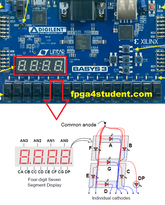
Last time, I presented an FPGA tutorial on how to control the 4-digit 7-segment display on the Basys 3 FPGA board. Full Verilog and VHDL code for displaying a 4-digit number on the 7-segment display of FPGA Basys 3 were also provided.

This FPGA tutorial tells you how to interface a mouse with Xilinx Basys 3 FPGA board. The FPGA tutorial also provides a Verilog code for interfacing a mouse with FPGA Basys 3.

How to interface a mouse with FPGA Basys 3

FPGA VHDL Online Course for Beginners

Last time, I recommended several cheap and good Xilinx or Altera FPGA boards for beginners or students. These FPGA boards are not only very affordable for students, but also provides good onboard devices such as LEDs, switches, buttons, 7-segment display, VGA, UART port, etc for beginners to practice many different basic projects.

Today, I present my recommended FPGA course for beginners and students to learn VHDL design on FPGA. The FPGA course has over 3,890 students and 430 good reviews. 

FPGA VHDL Courses

VHDL code for Seven-Segment Display on Basys 3 FPGA

Last time, I wrote a full FPGA tutorial on how to control the 4-digit 7-segment display on Basys 3 FPGA. A full Verilog code for displaying a counting 4-digit decimal number on the 7-segment display was also provided.

This VHDL project will present a full VHDL code for seven-segment display on Basys 3 FPGA. The seven-segment display on Basys 3 FPGA will be used to display a 4-digit hexadecimal number which is counting up every 1 second. 

VHDL code for Seven-Segment Display on Basys 3 FPGA

[FPGA Tutorial] Seven-Segment LED Display on Basys 3 FPGA

This FPGA tutorial will guide you how to control the 4-digit seven-segment display on Basys 3 FPGA Board. A display controller will be designed in Verilog for displaying numbers on the 4-digit 7-segment LED display of the Basys 3 FPGA. Full Verilog code for the seven-segment LED display controller will also be provided.

The Basys 3 FPGA has a common-anode 4-digit 7-segment LED display as shown in the following figure.

FPGA Tutorial - Seven-Segment LED Display Controller on Basys 3 FPGA

Full VHDL code for Moore FSM Sequence Detector

Last time, I presented a Verilog code together with Testbench for Sequence Detector using FSM. The sequence being detected was "1011". 

This VHDL project presents a full VHDL code for Moore FSM Sequence Detector. A VHDL Testbench is also provided for simulation. The sequence to be detected is "1001".

Full VHDL code for Moore FSM Sequence Detector

Full Verilog code for Moore FSM Sequence Detector

This Verilog project is to present a full Verilog code for Sequence Detector using Moore FSM. A Verilog Testbench for the Moore FSM sequence detector is also provided for simulation. 

The Moore FSM keeps detecting a binary sequence from a digital input and the output of the FSM goes high only when a "1011" sequence is detected. The state diagram of the Moore FSM for the sequence detector is shown in the following figure.
Full Verilog code for Moore FSM Sequence Detector

VHDL code for MIPS Processor

Last time, I presented a Verilog code for a 16-bit single-cycle MIPS processor. The instruction set and architecture design for the MIPS processor was provided here.

Today, the VHDL code for the MIPS Processor will be presented. A simple VHDL testbench for the MIPS processor will be also provided for simulation purposes.

VHDL code for MIPS Processor

Car Parking System in VHDL

This VHDL project presents a car parking system in VHDL using Finite State Machine (FSM). VHDL code and testbench for the car parking system are fully provided.

The VHDL car parking system is shown in the following figure. There is a front sensor to detect vehicles going to the gate of the car parking system. Another back sensor is to detect if the coming vehicle passed the gate and getting into the car park. 

Car Parking System in VHDL using Finite State Machine (FSM)

VHDL code for single-port RAM

This VHDL post presents a VHDL code for a single-port RAM (Random Access Memory). The VHDL testbench code is also provided to test the single-port RAM in Xilinx ISIM. The RAM's size is 128x8 bit.

VHDL code for a single-port RAM

VHDL code for Comparator

This VHDL project presents a simple VHDL code for a comparator which is designed and implemented in Verilog before. Full VHDL code together with test bench for the comparator is provided.

The design for the comparator based on the truth table and K-map are already presented here. There are two 2-bit inputs A and B to be compared. Three output signals are A_less_B (1 if A < B, else 0), A_equal_B (1 if A=B, else 0), and A_greater_B (1 if A>B, else 0). The minimized expressions obtained from K-Map tables for the outputs are used for VHDL coding of the comparator.

VHDL code for a comparator

Verilog code for PWM generator

This Verilog project presents a Verilog code for PWM generator with Variable Duty Cycle. Last time, I presented a VHDL code for a PWM generator.

The Verilog PWM (Pulse Width Modulation) generator creates a 10MHz PWM signal with variable duty cycle. Two buttons which are debounced are used to control the duty cycle of the PWM signal. The first push button is to increase the duty cycle by 10%, and the other button is to decrease the duty cycle by 10%. 

Verilog code for PWM Generator

VHDL code for Traffic light controller

A VHDL code for a traffic light controller on FPGA is presented. The traffic light controller in VHDL is used for an intersection between highway and farm way. 

There is a sensor in the farm way side to detect if there is any vehicle on the farm way. If vehicles are detected on the farm way, traffic light on the high way turns to YELLOW, then RED so that the vehicles from the farm way can cross the high way. Otherwise, the traffic light on the high way is always GREEN and traffic light on the farm way is always RED. The time period is 3 seconds for the YELLOW light and 10 seconds for the RED light. 

VHDL code for Traffic light controller

VHDL code for debouncing buttons on FPGA

When pressing buttons on FPGA, there are unpredictable bounces that are unwanted. This VHDL code is to debounce buttons on FPGA by only generating a single pulse with a period of the input clock when the button on FPGA is pressed, held long enough, and released. Last time, I presented a simple Verilog code for debouncing buttons on FPGA.

This VHDL project is to present a VHDL code for debouncing buttons on FPGA. Full VHDL code and testbench are provided.

VHDL code for debouncing buttons on FPGA

How to generate a clock enable signal on FPGA

This post is about to tell you how to generate a clock enable signal (not gated clocks) to drive another logic using the same clock domain instead of creating another clock (using clock dividers or clock gating) possibly causing FPGA timing issues (as created by non-dedicated FPGA clock generators) or clock domain crossing problems such as metastability, data loss, and data incoherency if it is not taken care. 
How to generate a clock enable signal instead of creating another clock domain

Verilog code for Clock divider on FPGA

Last time, I presented a VHDL code for a clock divider on FPGA. This Verilog project provides full Verilog code for the Clock Divider on FPGA together with Testbench for simulation. The Verilog clock divider is simulated and verified on FPGA.

Verilog code for Clock divider on FPGA

VHDL Code for Clock Divider on FPGA

This VHDL project presents a full VHDL code for clock divider on FPGA. Testbench VHDL code for clock divider is also provided. The VHDL code for the clock divider is synthesizable and verified on FPGA.

VHDL Code for Clock Divider on FPGA

Verilog vs VHDL: Explain by Examples

Last time, I presented in detail what actually FPGA programming is and how to get started with FPGA design. A brief history of Verilog and VHDL was also discussed. If you search for the difference between Verilog and VHDL, you will see many difference pages discussing this HDL language war, but most of them are short and not well-explained by examples for facilitating beginners or students' understanding.

The difference between Verilog and VHDL will be explained in detail by examples in this post. The advantages and disadvantages of Verilog and VHDL will be also discussed.

Verilog vs VHDL: Explain by Example

What is FPGA Programming?

Last time, I presented in detail what exactly an FPGA is and the advantage of FPGAs over ASICs and microcontrollers. FPGAs are nothing, but reconfigurable logic blocks and interconnects can be programmed by Hardware Description Language like Verilog/ VHDL to perform a specific functionality.

Today, I will present what actually FPGA programming is, how to get started with FPGA programming, and FPGA programming design flow. The difference between FPGA programming and software programming will be also discussed.

What is FPGA Programming?

Altera FPGA boards for beginners

Last time, I presented my four recommended and affordable Xilinx FPGA boards for beginners. The recommended Xilinx FPGA boards offer good enough number of IO devices and supporting circuits for student projects or practice, and more importantly, the FPGA boards are affordable for beginners or students.

In this FPGA post, I will present another four recommended and affordable Altera FPGA boards for beginners. These Altera FPGA boards are also very cheap and well-designed for students or beginners. 

1. Cyclone IV Altera FPGA Board from Aliexpress (33.69USD)

Recommended and affordable Altera FPGA boards for students

Xilinx FPGA boards for beginners

As a FPGA website for beginners or students, I always look for good and cheap Xilinx FPGA boards for beginners. There are many cheap Xilinx FPGA boards, but many of them are not easy to use especially for students or beginners; they do not offer onboard 7-segment LEDs, switches, LCD, RS232/ VGA port, other needed peripherals for beginners playing around with the board. Many FPGA boards from Xilinx are very user-friendly and they provide many onboard devices, but the price is not affordable for beginners.

Today, I will present my most recommended and affordable Xilinx FPGA development boards for beginners or students. These FPGA boards are affordable and offer all beginners need for their practice and academic projects. 

Verilog Code for Ripple Carry Adder

A Verilog code for a 4-bit Ripple-Carry Adder is provided in this project.

The 4-bit ripple-carry adder is built using 4 1-bit full adders as shown in the following figure.
Verilog code for ripple carry adder

Cryptographic Coprocessor Design in VHDL

In this VHDL project, the complete coprocessor for cryptographic applications is designed and implemented in VHDL. 

As mentioned in the previous Verilog/ VHDL projects, the coprocessor provideds standard instructions and dedicated function units specific for security. The co-processor is designed and implemented in VHDL, but the N-bit Adder in ALU unit is implemented in Verilog. 

The block diagram of the coprocessor is as follows:
Cryptographic Coprocessor Design in VHDL

Non-linear Lookup Table Implementation in VHDL

In this VHDL project, a nonlinear lookup table which is used in hashing functions of the upcoming co-processor is implemented in VHDL.

The nonlinear operation which is used in hashing algorithm utilizes a parallel 4-bit nonlinear operation where the input nibble (4 bits) are mapped to another nonlinear 4-bit value. 

The nonlinear lookup operation unit is shown in the following figure:
Non-linear Lookup Table Implementation in VHDL

Shifter Design in VHDL

In this VHDL project, a shifter with the ability to shift and rotate data, which is mainly used in the permutation and transpositions of ciphers, will be implemented in VHDL. The VHDL shifter is a key component in the upcoming co-processor's processing unit. Fast shifting and rotating functions are critical for cryptographic applications.

VHDL code for the shifter will be presented together with its testbench VHDL code for functional simulation.

VHDL code for Shifter

16-bit ALU Design in VHDL

Last time, I introduced the N-bit adder design in Verilog, which is a part of a 16-bit ALU design I will present today. The 16-bit ALU is a core combinational component of the processing unit in the coprocessor I introduced in the previous post.

Full VHDL code for 16-bit ALU together with testbench will be presented in this VHDL project. 

VHDL code for 16-bit ALU

N-bit Adder Design in Verilog

The next Verilog/ VHDL project is a complete co-processor specially designed for cryptographic applications. The co-processor has standard instructions and dedicated function units specific for security. The co-processor is implemented mainly in VHDL, but the N-bit Adder is designed in Verilog. The Verilog code for the N-bit Adder will be instantiated later in a VHDL design. In next posts, implementations of major modules in the co-processor will be presented. The complete co-processor design and implementation will be presented after every part of the co-processor is posted.

This post presents Verilog code for N-bit Adder designed for the co-processor. The Verilog code for N-bit Adder is done by using Structural Modeling. 

Verilog code for N-bit Adder using Structural modeling

Verilog code for Multiplexers

Multiplexers are one of the main combinational logic components in digital circuits. Multiplexers are used for selecting one of many different digital inputs and forwarding to the output based on the controlling signals. 

In this Verilog project, Verilog code for multiplexers such as 2-to-1 multiplexer, 2x5-to-5 multiplexer and 2x32-to-32 multiplexer are presented. 

Verilog code for multiplexer

Verilog code for Decoder

Decoder is one of the main combinational components in digital circuits. Decoders are mainly used in memory address decoding and data demultiplexing. 

In this Verilog project, Verilog code for decoder is presented. The decoder is used for memory address decoding.

verilog code for decoder

Pipelined MIPS Processor in Verilog (Part-3)

This project is to present the Verilog code for a 32-bit pipelined MIPS Processor. In part 2, I presented all the Verilog code for the single-cycle MIPS datapath. 

In this part, pipelined registers are added to complete the pipelined MIPS Processor. Verilog code for the complete 32-bit pipelined MIPS processor will be presented. 

Below is the complete data path for the 32-bit 5-stage pipelined MIPS Processor after adding Pipelined Registers, Forwarding Unit, Stall Control Unit, and Flush Control Unit to the single-cycle datapath. Forwarding, Stall Control, and Flush Control units are designed to solve data and control hazards in the pipelined MIPS processor. Following are the detailed explanation for the hazard-solving modules and the complete pipelined MIPS processor in Verilog.

verilog code for pipelined mips processor
Pipelined MIPS Processor Datapath

Pipelined MIPS Processor in Verilog (Part-2)

This project is to present the Verilog code for 32-bit 5-stage pipelined MIPS Processor

In part 1, I presented the instruction set of the pipelined MIPS processor and partially provided the Verilog code for the single-cycle MIPS datapath as shown below. Now, continue on the design and Verilog code for the ALU of the MIPS processor.


verilog code for pipelined mips processor
Single-Cycle MIPS Datapath

Pipelined MIPS Processor in Verilog (Part-1)

Last time, I posted a Verilog code for a 16-bit single-cycle MIPS Processor and there were several requests for a Verilog code of a 32-bit 5-stage pipelined MIPS Processor. The first problem with the single-cycle MIPS is wasteful of the area which only each functional unit is used once per clock cycle. Another serious drawback is that the clock cycle is determined by the longest possible path in the Processor. Thus, the pipelined MIPS came out to solve those problems by exploiting most functional unit in one clock cycle and improving the performance by increasing the instruction throughput. However, the pipelined MIPS also faces challenges such as control and data hazards.

Today, a 32-bit 5-stage pipelined MIPS Processor will be designed and implemented in Verilog

Verilog code for special modules such as Forwarding Unit, Flush Control Unit and Stall Control unit for solving hazards will be also provided. The Verilog code for 32-bit pipelined MIPS Processor is mostly done by using structural modeling.

This project is quite long so I will divide it into 3 parts (Part 1, Part 2, and Part 3).
verilog code for pipelined mips processor
Pipelined MIPS Design Flow

VHDL code for counters with testbench

Last time, several 4-bit counters including up counter, down counter and up-down counter are implemented in Verilog. Verilog code for the counters is presented. 

In this VHDL project, the counters are implemented in VHDL. The testbench VHDL code for the counters is also presented together with the simulation waveform. 


VHDL code for counter with testbench

Verilog code for Arithmetic Logic Unit (ALU)

Last time, an Arithmetic Logic Unit (ALU) is designed and implemented in VHDL. Full VHDL code for the ALU was presented. 

Today, fpga4student presents the Verilog code for the ALU. The testbench Verilog code for the ALU is also provided for simulation.


Verilog code for ALU

VHDL code for Arithmetic Logic Unit (ALU)

Arithmetic Logic Unit (ALU) is one of the most important digital logic components in CPUs. It normally executes logic and arithmetic operations such as addition, subtraction, multiplication, division, etc.

In this VHDL project, an ALU is designed and implemented in VHDL. VHDL code for the ALU is fully presented.

VHDL code for ALU

Tic Tac Toe Game in Verilog and LogiSim

Tic Tac Toe is a very popular paper-and-pencil game in a 3x3 grid for two players. The player who makes the first three of their marks in a diagonal, vertical, or horizontal row wins the game.

Today, fpga4student designs and implements the Tic Tac Toe game in Verilog and Logisim

Tic Tac Toe Game in Verilog and LogiSim

PWM Generator in VHDL with Variable Duty Cycle

Pulse Width Modulation (PWM) is a very popular modulation technique which is mainly used to control the power delivered to electrical devices such as motors.

This VHDL project presents a simple VHDL code for PWM Generator with Variable Duty Cycle. The VHDL code for PWM Generator is simulated and verified on Xilinx ISIM.


VHDL code for PWM Generator

How to write Verilog Testbench for bidirectional/ inout ports

This post describes how to write a Verilog testbench for bidirectional or inout ports. This happens in special designs which contain bidirectional or inout ports such as I2C core, IO pads, memories, etc. 

In this post, I will give an example how to write testbench code for a digital IO pad. Basically, the IO pad has logic inputs DS, OEN, IE, PE to configure the IO pad as an input or output. When DS = OEN = IE = PE = 1, the IO pad operates as an input pad. Thus, the data from the bidirectional port PAD are written into the output C. When DS = PE =1 and OEN = IE = 0, the IO pad operates as an output pad. Therefore, the signal from the input I is passed to the bidirectional port PAD.
Verilog testbench for bidirectional/ inout port

Verilog code for debouncing buttons on FPGA

This post is to present a simple debouncing Verilog code for buttons on FPGA. 

Mechanical switches/ buttons cause an unpredictable bounce in the signal when toggled. There are various ways to implement debouncing circuits for buttons on FPGA. In this project, a simple debouncing circuit is implemented in Verilog to generate only a single pulse when pressing a button on FPGA. 

Verilog code for button debouncing

Debouncing Circuit for buttons on FPGA

Verilog Code for 16-bit RISC Processor

In this Verilog project, Verilog code for a 16-bit RISC processor is presented. 

The RISC processor is designed based on its instruction set and Harvard-type data path structure. Then, the RISC processor is implemented in Verilog and verified using Xilinx ISIM.


Verilog code for RISC processor

Verilog code for counter with testbench

In this project, Verilog code for counters with testbench will be presented including up counter, down counter, up-down counter, and random counter.

Verilog code for counter with testbench

VHDL code for Full Adder

In this VHDL project, VHDL code for full adder is presented. VHDL code for the adder is implemented by using behavioral and structural models. 

The full adder has three inputs X1, X2, Carry-In Cin and two outputs S, Carry-Out Cout as shown in the following figure:

VHDL code for full adder

Verilog code for Full Adder

In this Verilog project, Verilog code for Full Adder is presented. Both behavioral and structural Verilog code for Full Adder is implemented. 

Verilog code for Full Adder

VHDL code for D Flip Flop

VHDL code for D Flip Flop is presented in this project. Verilog code for D Flip Flop here. There are several types of D Flip Flops such as high-level asynchronous reset D Flip-Flop, low-level asynchronous reset D Flip-Flop, synchronous reset D-Flip-Flop, rising edge D Flip-Flop, falling edge D Flip-Flop, which is implemented in VHDL in this VHDL project.

VHDL code for D Flip Flop

Verilog code for D Flip Flop

D Flip-Flop is a fundamental component in digital logic circuits. Verilog code for D Flip Flop is presented in this project. There are two types of D Flip-Flops being implemented which are Rising-Edge D Flip Flop and Falling-Edge D Flip Flop. 

Verilog code for D Flip Flop

Verilog code for a comparator

In this project, a simple 2-bit comparator is designed and implemented in Verilog HDL. Truth table, K-Map and minimized equations for the comparator are presented. The Verilog code of the comparator is simulated by ModelSim and the simulation waveform is presented.


Verilog code for a comparator

VHDL code for FIFO Memory

As requested by some readers, I made the VHDL code for the FIFO memory in this VHDL project(Verilog code for FIFO memory). 

The FIFO has 16 8-bit data-width stages and five status signals including overflow, underflow, empty, full and threshold. The VHDL code for the FIFO memory is verified by the same Verilog testbench code by doing a mixed language simulation on Xilinx ISIM. 

VHDL code for FIFO Memory

Verilog code for FIFO memory

In this project, Verilog code for FIFO memory is presented. The First-In-First-Out (FIFO) memory with the following specification is implemented in Verilog:

  • 16 stages
  • 8-bit data width 
  • Status signals: 
    • Full: high when FIFO is full else low.
    • Empty: high when FIFO is empty else low.
    • Overflow: high when FIFO is full and still writing data into FIFO, else low.
    • Underflow: high when FIFO is empty and still reading data from FIFO, else low.
    • Threshold: high when the number of data in FIFO is less than a specific threshold, else low.

Verilog code for FIFO memory

Verilog code for 16-bit single cycle MIPS processor

In this project, a 16-bit single-cycle MIPS processor is implemented in Verilog HDL. MIPS is an RISC processor, which is widely used by many universities in academic courses related to computer organization and architecture. 

The Instruction Format and Instruction Set Architecture for the 16-bit single-cycle MIPS are as follows:

Verilog code for 16 bit MIPS CPU
Instruction set for the MIPS processor

Delay timer (LS7212) in Verilog HDL

Today's project is an implementation of a programmable digital delay timer in Verilog HDL. Verilog code for the delay timer is fully presented.

Verilog code for delay timer

Basic digital logic components in Verilog HDL

In this Verilog project, basic blocks in digital logic design such as D-Flip-Flop, adders, ALU, registers, memory, multiplexers, decoders, counters, etc.  are implemented in Verilog HDL for beginners.

Verilog code for MIPS processor

Popular FPGA/Verilog/VHDL Projects