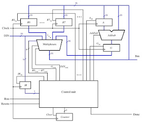
A 16-bit CPU design in Logisim is presented. The 16-bit simple CPU with data-path and control unit is shown as below:

The design process for the CPU in Logisim:
1. Multiplexers:

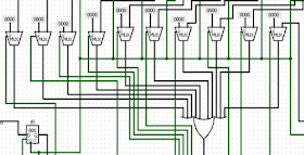
Figure 2. The screenshot of multiplexers
In this design, multiplexers module will get the 10-bit select signal from control unit and output the one of 10 16-bit data input. To design this module, we can see that the multiplexer will transfer the Nth 16-bit data input to the output if the Nth bit of the 10-bit select signal is asserted “HIGH” and other bits are zero. It is note that the select signal from controller unit should be controlled like this. There is just one bit of the 10-bit select signal which is high at a moment. For example, if we want the multiplexer to output the 4th input, the select signal will be 0x008 = 0000001000.
Thus, we use 10 multiplexers 2 to 1 with the 1-bit select signal in 10-bit input from control unit at the first stage of the module. Each multiplexer will output the input data if the 1-bit select signal is high, otherwise it will output zero. Then at the 2nd stage, we use a OR gate to OR all the outputs of 10 multiplexers. Since there is just 1 bit in the 10-bit select signal is asserted HIGH, we will get the expected output at the output of the OR gate.
The Bus Output = Dout when DinOut is asserted HIGH.
The Bus Output = R0in…R7in when R0out….R7out is asserted HIGH
The Bus Output = Gin when Gout is asserted HIGH
2. Addsub:

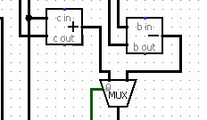
Figure 3. The screenshot of Addsub module
This module will perform the ADD and SUB operation according to the addsub signal from the controller unit. The MUX will choose the result of which operation in the following:
Addsub = 0 : it perform ADD operation.
Addsub = 1 : it perform SUB operation.

Figure 4. The screenshot of 2-bit counter module
The 2-bit counter will be up according to the rising-edge of clock and clear to zero if run = 0 or Resetn = 0. Thus, we use 2 T-Flip Flop and connect to each other like in figure 4 and the OR gate is used to generate the clear signal in order to clear the counter.
Brief about T Flip-Flop :

Function: If the T input is high, the T flip-flop changes state ("toggles") whenever the clock input is rising-edge. If the T input is low, the flip-flop holds the previous value. This behavior is described by the characteristic equation:
Qnext = T xor Q
To make it as a counter, the T input is asserted HIGH. It becomes Qnext=not Q. We connect 2 T-FFs in the following diagram:

Figure 5. 2-bit up counter using TFF
Operation

Table 1. Operation of 2-bit up counter using TFF
b. Control Unit:

Table 2. Control signals
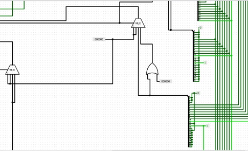
We will design the control unit based on the table above. It can be seen that in the first cycle the IRin will be asserted HIGH, and the next cycles the control signals are follow the table. The number of cycles will equal the value of 2-bit counter, so we will get the output of counter to be the select signal for multiplexer at the final stage of the control unit in the figure below.

Figure 6. The screen shot of the final stage of control unit
Also, the MUX 2 to 1 in the image above is used to clear all the control signals when the Resetn is asserted LOW.
Besides, from the table, in each cycle we need a MUX 4 to 1 to select the control signal for 4 different instructions, so we use 3 MUX 4 to 1 for 3 cycles and each input of the 3 MUX 4 to 1 depends on the value of IR from 8th to 6th. The details are as follows:

Figure 7. The screenshot of part 1 of 3 MUX 4 to 1

Figure 8. The screenshot of part 2 of 3 MUX 4 to 1
As we can see that we use 2 decoder 3 to 8 to decode the register address. The first one is to decode 3 bit RX to 8-bit control signal, the other one is to decode 3 bit RY to 8-bit control signal.
Finally, we follow the table 2 to feed the right inputs for 3 MUX 4 to 1 according to the instructions and number of cycles. Details in the figure 7 and 8.
4. The 16-bit simple CPU in Logisim
We connect all the modules before and registers to achieve the circuit file simple_CPU.circ and tested using Logisim.

Figure 9. The final circuit

Figure 10. The control unit circuit including the counter module
The 16-bit CPU circuit is tested successfully the final circuit on Logisim by changing various Din or instructions and observing the value of Bus, register file and control signals.
Logisim Circuit file Download:
You might also like this:
VHDL code for D Flip Flop
Verilog code for D Flip Flop
Verilog code for a comparator
Verilog code for FIFO memory
VHDL code for FIFO memory
Verilog code for 16-bit single-cycle MIPS microprocessor
Programmable digital delay timer in Verilog
Basic digital logic components in Verilog HDL
FIR Filter in VHDL
What is an FPGA? Why FPGA?
A complete 8-bit Microcontroller in VHDL
Verilog code for 32-bit unsigned Divider
Fix-point matrix multiplication in Verilog[Full code and tutorials]
Verilog code for a Carry Look Ahead Multiplier
Verilog code for a microcontroller (Part-3)
16-bit Processor CPU design and implementation in LogiSim
Image processing on FPGA using Verilog HDL
Parameterized N-bit switch tail ring counter
Verilog code for 4x4 Multiplier using two-phase self-clocking system
VHDL code for digital clock on FPGA
Verilog code for a parking system using Finite State Machine (FSM)
Verilog code for Traffic light controller
Verilog code for Alarm clock on FPGA
VHDL code for the 8-bit Comparator
Matrix Multiplication Design using VHDL and Xilinx Core Generator
Two ways to load a text file into FPGA
Plate License Recognition Verilog/Matlab Implementation on FPGA Xilinx Spartan-6
What is FPGA Programming? FPGA vs Software programming
Recommended and affordable Xilinx FPGA boards for students
Recommended and affordable Altera FPGA boards for students
N-bit Adder Design in Verilog
Verilog vs VHDL: Explain by Examples
Verilog code for PWM Generator
Verilog coding vs Software Programming
Single-cycle MIPS processor in VHDL
Verilog vs VHDL: Explain by Examples
Verilog code for PWM Generator
Verilog coding vs Software Programming
Single-cycle MIPS processor in VHDL


No comments:
Post a Comment